
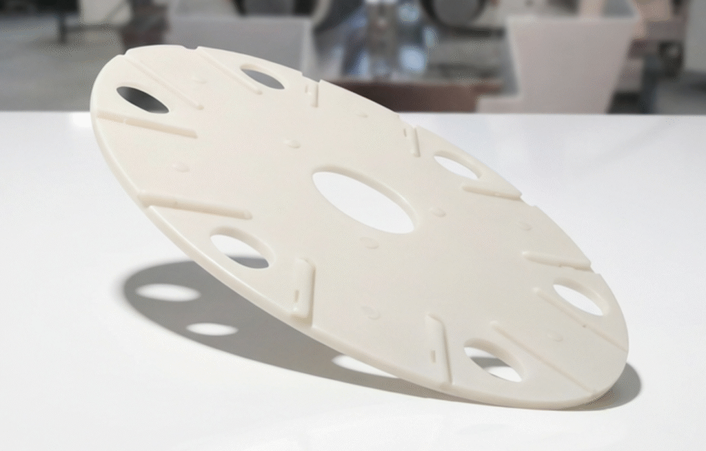
Engineers designing thermal management for power modules have likely noticed recently that as SiC and IGBT devices push higher voltages and currents, the substrate’s heat dissipation becomes the bottleneck. Aluminum nitride (AlN) ceramics—with a thermal conductivity of 170–230 W/(m·K), a CTE of 4.5×10⁻⁶/K matching silicon, and electrical insulation—should be the star student on paper. But once you get to the drilling step, procurement and process engineers start getting headaches: chipping, micro-cracks, rough hole walls, positional deviation—the problems come one after another.
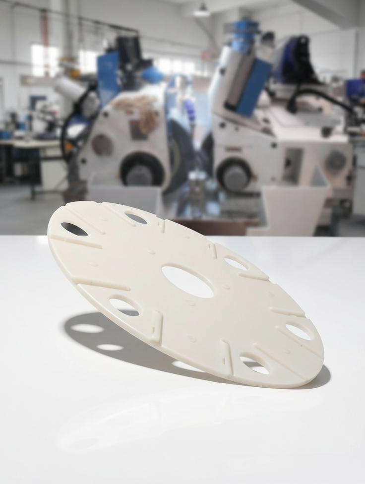
I. First, Understand This: Why Is Drilling AlN So Difficult? Let’s Go Back to the Material Physics
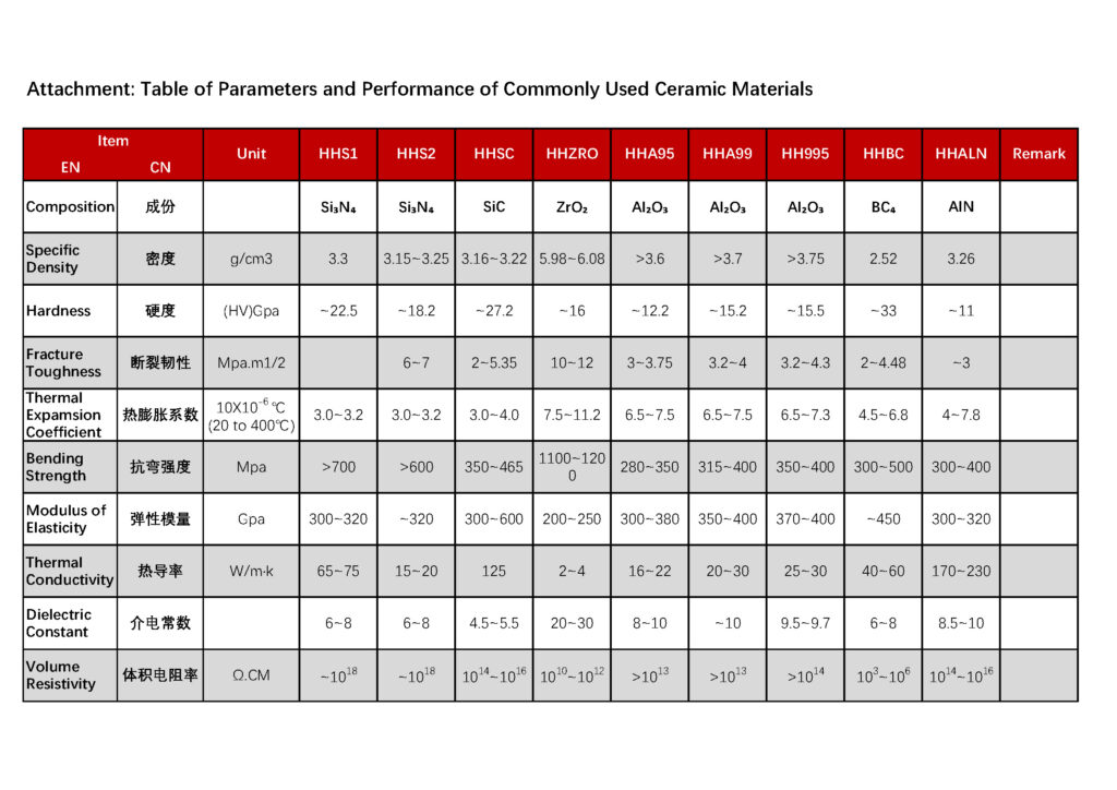
After sintering, AlN has a Vickers hardness of ~11 GPa, flexural strength of 350–450 MPa, and fracture toughness of only 2.4–3.0 MPa·m¹/²—a textbook example of hard-brittle material removal at the microscale. Add to that the fact that AlN slowly hydrolyses in water (AlN + H₂O → Al(OH)₃ + NH₃)—prolonged wet processing turns the surface white, requiring rework before metallization. With these properties stacked together, the drilling process must find a balance between “hard-on-hard” contact and thermal damage:
- Mechanical drilling (PCD/diamond): Low cost, good metallization affinity on hole walls, but chipping is hard to control—especially exit-side chipping on thin substrates (<0.635 mm).
- Laser (UV/picosecond/femtosecond): Non-contact, excellent absorption of ultrafast laser by AlN; chipping can be suppressed to within 20 μm, aspect ratio up to 1:10, but slag and recast layers require post-processing. Water-jet-guided laser is even more aggressive—130 holes of φ0.5 mm in a 0.61 mm thick plate can achieve zero chipping and zero carbonisation.
- Workaround methods like “leaving margin on the back side and grinding it off” or “double-sided drilling” can salvage parts, but they waste material and time—not economical for batch production.
II. Without Quantifying the Four Operating Parameters, Adjusting Process Settings Is Like Feeling for an Elephant in the Dark
Many factories only tweak spindle speed and feed rate when drilling. In reality, AlN drilling involves four competing factors—temperature, stress, medium, and cycle count—which must be analyzed separately:
- Temperature Field: The cutting zone can spike locally to 800–1000°C. Although AlN has good thermal conductivity, the ceramic itself has limited heat dissipation paths. Frictional heat between the tool and workpiece can’t escape, creating a temperature differential of 300–400°C that generates thermal stress micro-cracks. These are invisible to the naked eye but degrade subsequent thermal conduction efficiency.
- Stress State: Thin-walled parts warp easily under even slightly excessive clamping force. Vacuum chucking is generally kept stable at -0.06 to -0.08 MPa—more restrained than the -0.1 MPa used for alumina.
- Medium Environment: Wet processing must guard against hydrolysis. Prolonged immersion causes AlN surface whitening, so dry machining or minimal quantity lubrication is more common.
- Cycle Count: Essentially the number of “layered cutting” passes—for a blind hole 0.2 mm deep, dividing it into 4 layers of 0.05 mm each with 10–15 seconds of interlayer pause for stress relief can tighten hole depth deviation from ±0.004 mm to ±0.002 mm. This is especially critical for array holes in batch production.
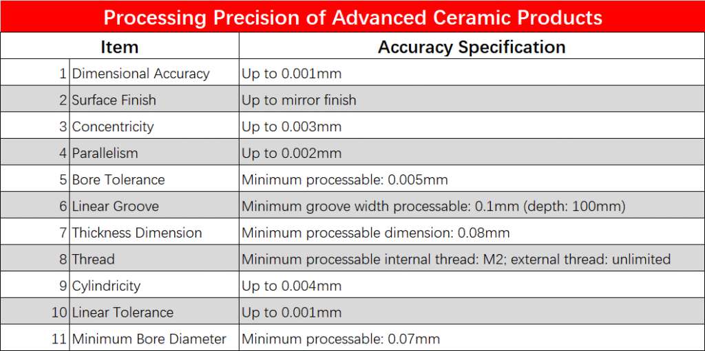
For reference, here are the typical tolerance ranges accepted in the industry for AlN substrates:
- Hole diameter φ0.2–2.0 mm: ±0.05 mm
- Hole centre distance: ±0.05 mm
- Minimum distance from hole edge to substrate edge: ≥1.2× substrate thickness and ≥1.0 mm
- Entry/exit diameter difference for through-holes: ≤8% of substrate thickness
III. Market Signals Are Actually More Urgent Than Process Challenges
This isn’t to say process doesn’t matter—it’s that demand-side pressure is already forcing the issue. Different research agencies’ data vary slightly, but the direction is consistent:
- Global AlN ceramic substrate market: China’s production value share reached 49.0% in 2024, surpassing Japan (42.9%).
- Per YH Research: Market scale projected to reach $280 million by 2031, CAGR 6.6%.
- Per Marketintelo (more aggressive estimate): $1.2 billion in 2024, rising to $2.85 billion by 2033, CAGR 10.1%.
- Downstream breakdown: Power electronics ~49%, LED packaging ~31%, automotive electronics ~20%. SiC modules, 800V fast charging, and 5G/6G RF are the main growth drivers.
Domestically, companies like Fujian Huaqing, Wuxi Haigude, and Zhuzhou Aisenda are chasing the market share of Japanese leaders Maruwa and Kyocera. But in the high-end segment of AMB+DPC combined AlN substrates with precision drilling, delivery lead times and technical responsiveness remain the most agonising factors for customers considering supplier switches.
IV. Delivery Reality: Can Small-Batch Sampling Scale Smoothly to Mass Production?
Going back to the chipping problem mentioned at the start. Based on the AlN drilling orders Shenzhen Xinluo Technology Co., Ltd. has handled in recent years, what customers care about most isn’t how small a single hole can be made, but whether three things can be stabilised simultaneously:
- Whether the technical handoff from drawing → sample → mass production can keep pace with revision cycles (power module customers changing package layouts is routine).
- Whether micro-hole arrays (φ0.2–1.0 mm) in thin substrates below 0.635 mm can keep chipping at the 20 μm level and positional deviation within ±0.05 mm.
- Whether the material specification aligns with the upstream sintering batch’s thermal conductivity grade (170/200/230 W/(m·K)), avoiding the discovery that the wrong substrate grade was selected after drilling is complete.
The current process strategy is primarily ultrafast laser with PCD mechanical drilling as a supplement—femtosecond laser for micro-hole arrays and irregular contours; PCD for holes requiring subsequent copper plating to preserve metallization affinity. Water-jet-guided laser is also beginning to enter the picture for ultra-thin substrates (<0.5 mm) and high-density micro-hole applications.
💡 An easily overlooked detail: Applying a stress-absorbing layer (wax/tape) before drilling AlN substrates, followed by ultrasonic cleaning to remove micro-crack debris—these two steps seem trivial, but they can boost batch yield from 85% to over 95%. They’re the “small leverage points in the process.”
V. Looking Ahead: The Real Value Lies in “Integration Capability,” Not Single-Point Parameters
Over the next two to three years, the competitive frontier for AlN drilling won’t be “who can make a φ0.1 mm micro-hole”—everyone can catch up on that with ultrafast lasers. The real differentiator will be coordination with the three downstream processes: AMB copper cladding, DPC electroplating, and DBC. Questions like: How should the drilling tolerance band be set so that subsequent copper climbing the hole wall doesn’t create voids? How should irregular hole arrays be arranged so that stress during SiC chip attachment doesn’t concentrate at corners?
These challenges can’t be solved by the substrate manufacturer alone or by the machining shop alone—engineers from both sides need to sit at the same table and review the drawings together. Shenzhen Xinluo Technology Co., Ltd.‘s current positioning leans in this direction—not selling on “how small the hole diameter is,” but making “drilling parameters aligned with the customer’s package roadmap” the delivery standard. After all, on the SiC module side, a chipped substrate edge or a hole position shifted by 0.03 mm can, after two reflow soldering cycles, become the root cause cited in a failure analysis report.
If you have AlN substrate drilling drawings on hand (thickness, hole array pattern, aspect ratio, whether metallization is required afterwards), start by filling in the four operating parameters table. Compare the results, then decide between laser and PCD. That approach is far more efficient than asking, “How much per hole?”
About Xinluo Ceramic:
Shenzhen Xinluo Technology Co., Ltd. (Xinluo) specialises in researching and developing all kinds of ceramic components, including Zirconia, Alumina, AlN, SiC, Si3N4 and mixed powder, as well as manufacturing. With an extensive selection of advanced ceramic materials and precision machining capabilities, we can deliver customised components with speed and accuracy. Depending on the application, Xinluo can help provide solutions for different materials.
Product Information: https://xinluoceramic.com/product-tag/material/
