Have you noticed the following phenomena in modern life?
- High-power new energy electric control units are continuously shrinking in size yet remain stable and durable under prolonged full-load operation. What exactly keeps their operating temperature in check?
- With the highly integrated design of high-frequency semiconductor devices, how do they achieve compact form factors that don’t overheat, get damaged, and have longer lifespans?
- Traditional, common ceramic materials have long fallen behind the pace of high-end electronics development. What new materials are breaking through technologically?
Many are puzzled. Electronic products are becoming increasingly compact and elegant, yet their integrated functionalities are becoming more complete and powerful. This industrial revolution of simultaneous miniaturisation and performance enhancement is, in fact, fundamentally driven by high-density integrated components.
While the external dimensions appear to simply get smaller, the internal industrial materials have already undergone generational upgrades. Today, we will plainly explain the thermal dissipation challenges behind the miniaturisation of electronic equipment and the high-end ceramic substrates that are providing the solution!
The Rise of High-Density Integration and the Thermal Challenge
The electronics industry is persistently iterating towards lighter, smaller, and smarter products. High-density integration of electronic components has become the mainstream trend. While integration levels have dramatically increased, the power density of devices continues to climb. This concentrates heat dissipation from component operation, frequently leading to issues like excessive overall temperature rise and thermal stress imbalance.
Thermal management has thus become the core bottleneck restricting the service life, operational stability, and safety of high-power electronic devices. Consequently, high-performance thermal dissipation substrates for electronic packaging have become a critical, rigid demand for industry chain upgrades.
Comparison of Mainstream Ceramic Packaging Substrates
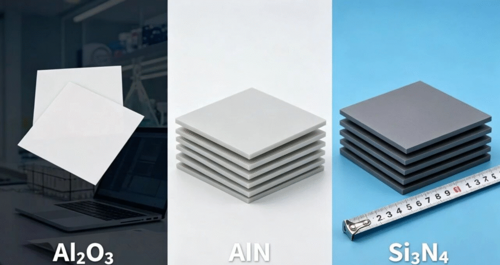
Currently, industrially mass-produced ceramic packaging substrates are mainly divided into three categories: Alumina (Al₂O₃), Aluminum Nitride (AlN), and Silicon Nitride (Si₃N₄). A comparison of their key performance metrics is shown in Figure 1.
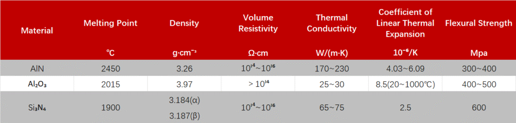
(Figure 1: Ceramic Substrate Material Performance Comparison Table)
- Alumina Substrates: Holding over 70% market share, they are the primary ceramic material for mid-to-low-end electronic packaging applications. This material offers excellent cost-performance, balanced properties, a thermal cycling life of about 200-300 cycles, and mature processing. It is widely used in DBC (Direct Bonded Copper) applications. However, limited by its inherently low thermal conductivity, it has weak heat dissipation capability and average thermal stability, making it unsuitable for high-power, high-heat-flux-density devices.
- Aluminium Nitride Substrates: They offer excellent thermal conductivity, and their coefficient of thermal expansion closely matches semiconductor materials like Si, SiC, and GaN, effectively reducing thermal stress. This makes them the preferred material for mid-to-high-end, high-power electronic packaging, widely used in DPC (Direct Plated Copper) and AMB (Active Metal Brazing) high-end packaging processes.
- Silicon Nitride Substrates: They possess extremely high mechanical strength, excellent high-temperature resistance, and superior insulation. Their thermal shock resistance life is 15~20 times that of aluminium nitride. However, the material is difficult to machine, and its manufacturing process is complex. Mass production relies on stringent sintering equipment like Hot Isostatic Pressing (HIP), with high temperature and pressure thresholds, leading to persistently high overall manufacturing costs. This is also the core bottleneck currently limiting its large-scale commercialisation for civilian industries.
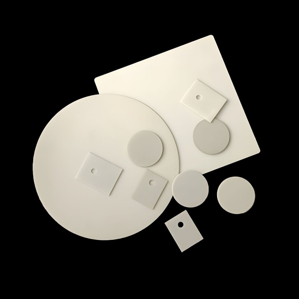
(Figure 2: Schematic Diagram of Ceramic Packaging Substrates)
Key Performance Parameters of Aluminium Nitride Substrates
The industry typically grades aluminium nitride substrates based on thermal conductivity. Mainstream commercial grades are 170 W/(m·K), 200 W/(m·K), and 230 W/(m·K). For high-end applications like high-power IGBT modules and ultra-high-density packaging devices, substrate thermal conductivity requirements have surpassed 200 W/(m·K).
Currently, leading domestic material companies have achieved mass production of ultra-high thermal conductivity aluminium nitride substrates at 250 W/(m·K), with technical standards comparable to international first-tier manufacturers.
Beyond thermal conductivity, high-quality aluminium nitride substrates have several other stringent control parameters:
- The coefficient of thermal expansion must be strictly controlled between 4.5 ~ 5.0 × 10⁻⁶/K.
- Flexural strength should be no less than 400 MPa.
- Dielectric breakdown strength should consistently exceed 15 kV/mm.
For the industry’s mainstream thick-film sintering process, substrate surface roughness and warpage are critical quality control points. The common industry standard requires Ra < 0.5 µm. Substrates with excellent flatness can significantly improve thick-film paste adhesion and printing accuracy, avoiding defects in the packaging process.
Sintering Processes for Aluminum Nitride
Mainstream AIN Sintering Processes:
There are generally five common sintering processes for AIN substrates in the industry: Hot Pressing (HP), Pressureless Sintering (PLS), Microwave Sintering, Spark Plasma Sintering (SPS), and Self-propagating High-temperature Synthesis (SHS). Among these, Hot Pressing is currently the primary process for preparing high thermal conductivity, dense AIN ceramics.
- Pressureless Sintering: Features low production costs and high capacity, suitable for mass-producing mid-to-low thermal conductivity (170~200 W/(m·K)) AIN substrates. It is the mainstream process for general-purpose commercial packaging substrates.
- Microwave Sintering & Spark Plasma Sintering: Characterised by fast heating rates and high sintered density. Mostly used for laboratory R&D and small-batch production of high-end samples. Equipment costs are high, making them unsuitable for large-scale mass production currently.
- Self-propagating High-temperature Synthesis features low energy consumption and fast reaction speed. However, the density consistency of the final product is poor, resulting in extremely low adoption rates for industrial mass production.
- Hot Pressing Sintering: Leveraging the synergistic effect of high temperature and high pressure, it can effectively eliminate internal pores in the green body, suppress impurity precipitation at grain boundaries, and maximise the purity of the aluminium nitride lattice. The final product offers stable thermal conductivity, high density, and excellent mechanical properties. It is the core manufacturing process for ultra-high thermal conductivity (230 W/(m·K) and 250 W/(m·K)) aluminium nitride substrates. However, this process suffers from high mould wear, limited batch capacity per furnace, and overall production costs higher than those of pressureless sintering. It is primarily used in high-value fields like high-end power semiconductors and aerospace.
About Us:
Xinluo Technology Co., Ltd. (Xinluo) specialises in researching and developing all kinds of ceramic components, including Zirconia, Alumina, AlN, SiC, Si3N4 and mixed powder, as well as manufacturing. With an extensive selection of advanced ceramic materials and precision machining capabilities, we can deliver customised components with speed and accuracy. Depending on the application, Xinluo can help provide solutions for different materials.
James Lin (Marketing Director)
Email: james@xinluoceramic.com
Tel/WhatsApp: +86-191-2995-4231
Product Information: https://xinluoceramic.com/product-tag/aluminum-nitride-aln/
Keyword:
#Aluminum Nitride Substrate
#AlN Ceramic Substrate
#High Thermal Conductivity Ceramic Substrate
#Electronic Packaging Substrates
#Advanced Ceramic Materials
#Aluminium nitride tape casting process
#AlN ceramic thermal conductivity 230W/mK
#Comparison of AlN vs Alumina vs Silicon Nitride substrates
#Ceramic substrates for high-power IGBT modules
#Thermal management for high-density electronic packaging
#Hot-press sintering for high-performance AlN ceramics
FAQ:
Q: What is the benefit of AlN substrates in IGBT modules?
Q: How does the sintering process affect the thermal conductivity of AlN?